A full wave rectifier circuit along with the output is shown in figure. The…
Physics · JEE Advanced · NTA Exams — Electronic Devices
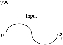
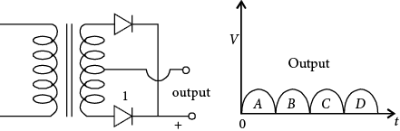
A full wave rectifier circuit along with the output is shown in figure. The contribution(s) from the diode 1 is (are)
- C
- A, C
- B, D
- A, B, C, D.
Answer
(B) A, C
Sign up free on Edukali to view the step-by-step worked solution and practice thousands of similar questions.
Related practice questions
- A Ge specimen is doped with Al. The concentration of acceptor atoms is ~10 21 atoms/m 3 . Given that the…
- In the following common emitter configuration an NPN transistor with current gain β = 100 is used. The output…
- A gate has the following truth table P 1 1 0 0 Q 1 0 1 0 R 1 0 0 0 The gate is
- A silicon specimen is made into a P- type semi-conductor by doping, on an average, one Indium atom per 5 × 10…
- The dominant mechanisms for motion of charge carriers in forward and reverse biased silicon p-n junctions are
- In the circuit given below, V(t) is the sinusoidal voltage source, voltage drop V AB (t) across the…
- In the circuit, if the forward voltage drop for the diode is 0.5 V , the current will be
- For a given plate voltage, the plate current in a triode value is maximum when the potential of
More Electronic Devices questions · Browse all practice questions