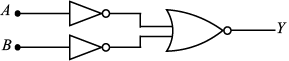
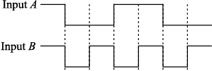
The logic circuit shown below has the input waveforms A and B as shown. Pick out the…
Physics · Class 12 · CBSE — Semiconductor Electronics
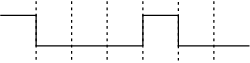
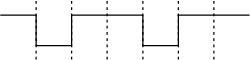
The logic circuit shown below has the input waveforms A and B as shown. Pick out the correct output waveform.
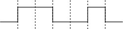
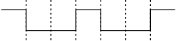
Answer
(A)
Sign up free on Edukali to view the step-by-step worked solution and practice thousands of similar questions.
Related practice questions
- The formation of depletion region in a p-n junction diode is due to
- A semiconductor has equal electron and hole concentration of 6 × 10 8 per m 3 . On doping with certain…
- The given graph represents the I-V characteristics of a Zener diode. Which part of the characteristics curve…
- For the forward biasing of a p-n junction diode, which of the following statements is not correct?
- A p - n photodiode is made of a material with a band gap of 2 eV. The minimum frequency of the radiation that…
- p -type semiconductors are formed when Si or Ge are doped with
- In case of a p-n junction diode at high value of reverse bias, the current rises sharply. The value of…
- Choose the only false statement from the following: In conductors the valence and conduction bands overlap…
More Semiconductor Electronics questions · Browse all practice questions