In the given Fig., V o is the potential barrier across a p-n junction, when no battery is…
Physics · Class 12 · CBSE — Semiconductor Electronics
In the given Fig., Vo is the potential barrier across a p-n junction, when no battery is connected across the junction
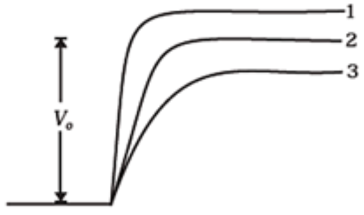
- 1 and 3 both correspond to forward bias of junction
- 3 corresponds to forward bias of junction and 1 corresponds to reverse bias of junction
- 1 corresponds to forward bias and 3 corresponds to reverse bias of junction.
- 3 and 1 both correspond to reverse bias of junction.
Answer
(B) 3 corresponds to forward bias of junction and 1 corresponds to reverse bias of junction
Sign up free on Edukali to view the step-by-step worked solution and practice thousands of similar questions.
Related practice questions
- Assertion (A): The impurities in p-type Si are not pentavalent atoms. Reason (R) : The hole density in…
- In an extrinsic semiconductor, the number density of holes is 4 10 20 m -3 . If the number density of…
- If a small amount of antimony is added to germanium crystal
- The following table provides the set of values of V and I obtained for a given diode. Let the characteristics…
- Suitable impurities are added to a semiconductor depending on its use. This is done to
- If a small amount of antimony is added to germanium crystal
- Assertion (A): Silicon is preferred over germanium for making semiconductor devices. Reason (R): The energy…
- The output current I versus time (t) curve of a full wave rectifier is shown in the figure. The average value…
More Semiconductor Electronics questions · Browse all practice questions